Spehro Pefhany
2021-07-17 04:23:58 UTC
Is there any kind of 'bible' reference for semi-automated test fixture
design or is all this stuff embedded in supplier data and internal
company lore?
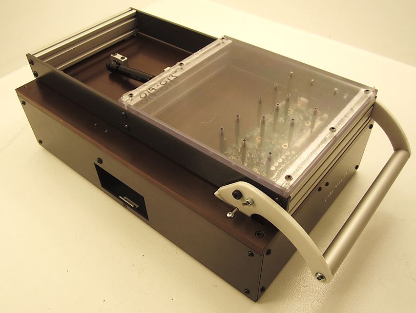
This kind of thing: Loading Image...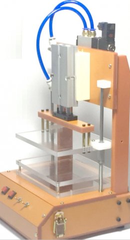 (pneumatic
actuated bed-of-nails)
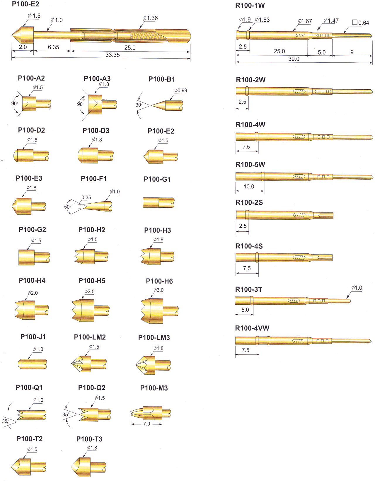
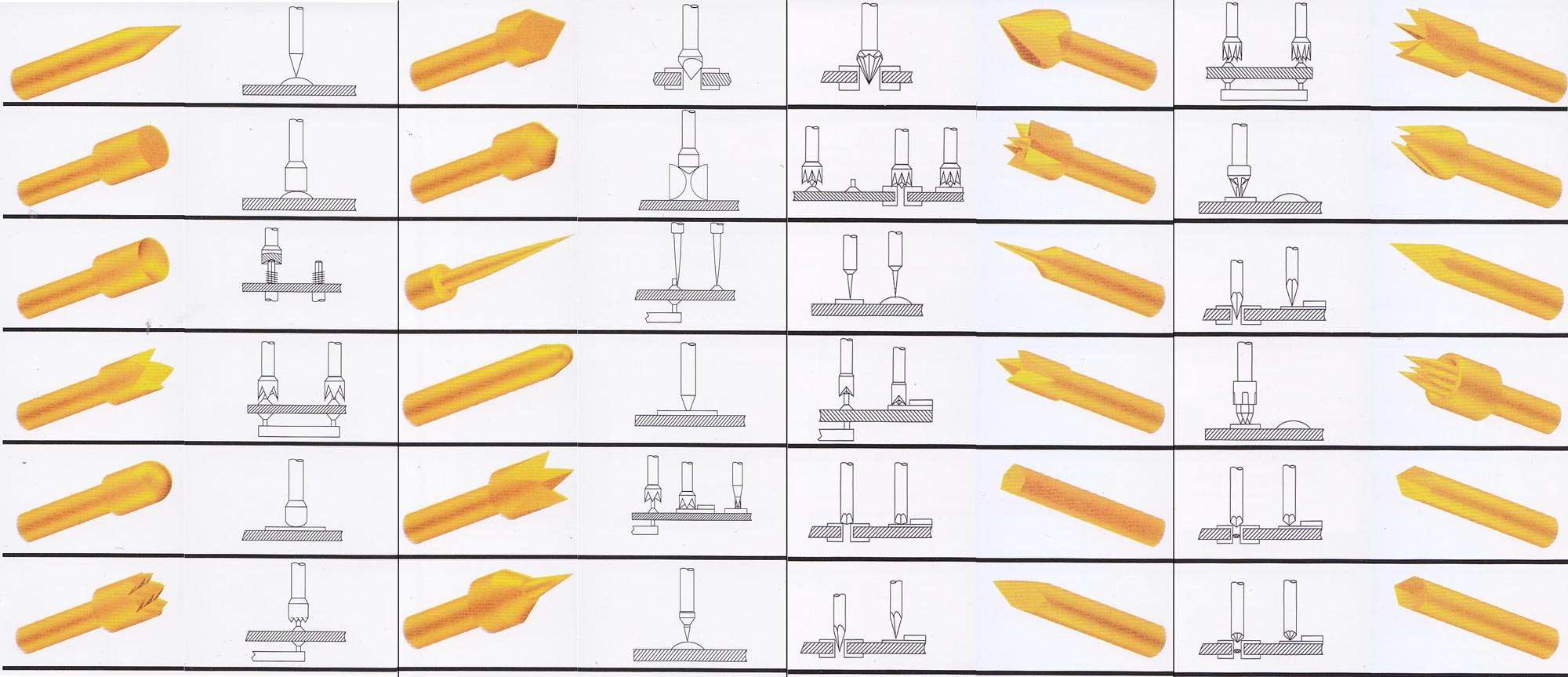
Primarily interested in the mechanical part of the design such as
location tolerances and location features on the PCB, and test pad
sizes using the common sizes and end details of pogo pins etc.
I've found a few things llike this:
https://circuitcheck.com/wp-content/uploads/2019/04/Design_Guide_Introduction_to_Automated_Test_Fixtures.pdf
https://www.testfixtures.com/pcb-test-fixtures/
https://resources.altium.com/sites/default/files/uberflip_docs/file_1215.pdf
This is going to be a stand-alone unit.
design or is all this stuff embedded in supplier data and internal
company lore?
This kind of thing: Loading Image...
 (pneumatic
actuated bed-of-nails)
Primarily interested in the mechanical part of the design such as
location tolerances and location features on the PCB, and test pad
sizes using the common sizes and end details of pogo pins etc.
I've found a few things llike this:
https://circuitcheck.com/wp-content/uploads/2019/04/Design_Guide_Introduction_to_Automated_Test_Fixtures.pdf
https://www.testfixtures.com/pcb-test-fixtures/
https://resources.altium.com/sites/default/files/uberflip_docs/file_1215.pdf
This is going to be a stand-alone unit.
--
Best regards,
Spehro Pefhany
Best regards,
Spehro Pefhany